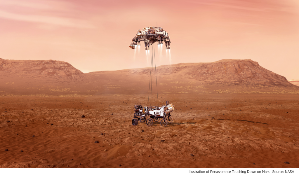
In February of 2021, the NASA Perseverance rover actively navigated a fully-autonomous entry and descent to successfully land in the Jezero Crater on Mars, using a brand-new navigational system developed by NASA – Terrain-Relative Navigation. The delay between mission control and the rover was about 11 minutes so a human-guided remote landing was not possible. Previous missions had to rely on known data to choose their landing spots, which meant they were chosen not for their scientific value but because they offered a higher probability of a successful landing.
But all that changed with the Perseverance and NASA’s Terrain-Relative Navigation. The rover navigated to the surface by comparing images of the terrain to images stored onboard, utilizing landmarks for orientation and navigation. These images were taken by seven cameras, mounted on both the rover and the entry vehicle, enabling the Perseverance to land on an entirely new area of Mars. And inside of these cameras were highly sensitive image sensors.
The story of image sensors has historically been very closely tied to photography, and often to the cameras in our phones. The evolution of phones, with slo-mo, portrait mode and macro options, has occurred over a relatively short period of time, giving every user the tools to create incredible imagery with a device that fits right in their pocket.
But the applications that use image sensors are expanding all the time and many times their purpose is not to capture images but to extract information from the environment. Applications that include:
- Smart retail where an image sensor might be part of a system that creates metadata based on consumer shopping and preferences
- Automotive where image sensors are part of the advanced driver assistance systems (ADAS) and eventually fully autonomous driving
- Medical imaging providing the ability to create smaller, more powerful devices to improve research, diagnoses, and medical procedures
- Augmented reality where image sensors are used for optical tracking
- Security where cameras are used for facial recognition technology
- Vision systems for robotics, automation, and other applications
- Food inspection where shortwave infrared sensors can detect and categorize food quality based on the image
The Image Sensor Market Is Primed for Significant Growth

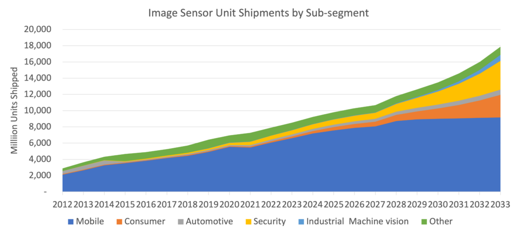
As image sensor applications have increased so have the number of units shipped. On the graph above, you can see that mobile has historically accounted for the largest percentage of units shipped, and that will continue. However, the graph also illustrates that consumer and security application shipments will increase exponentially over the next ten years.
One driver for the growth in mobile is the increase in the number of cameras and the camera resolution, as phone companies compete to deliver better, higher quality images. Consumers want to be able to zoom in on that concert performer or favorite player on the field and capture an image they can show their friends.
Add to that that the number of image sensors in the phone is also increasing. So even though total annual phone sales have plateaued, the number of image sensors in phones is expected to increase by 50% between now and 2027, with the complexity also continually increasing.
With this increase in units shipped, the segment’s revenue is projected to increase by 50% by the end of 2026. This growth in the market will draw increased investments from large established players and new entrants, and the variety and number of image sensors will increase. However, to ensure only high-quality sensors make it to end user devices, they must be tested.
Increasing Complexity Is Driving Test Challenges

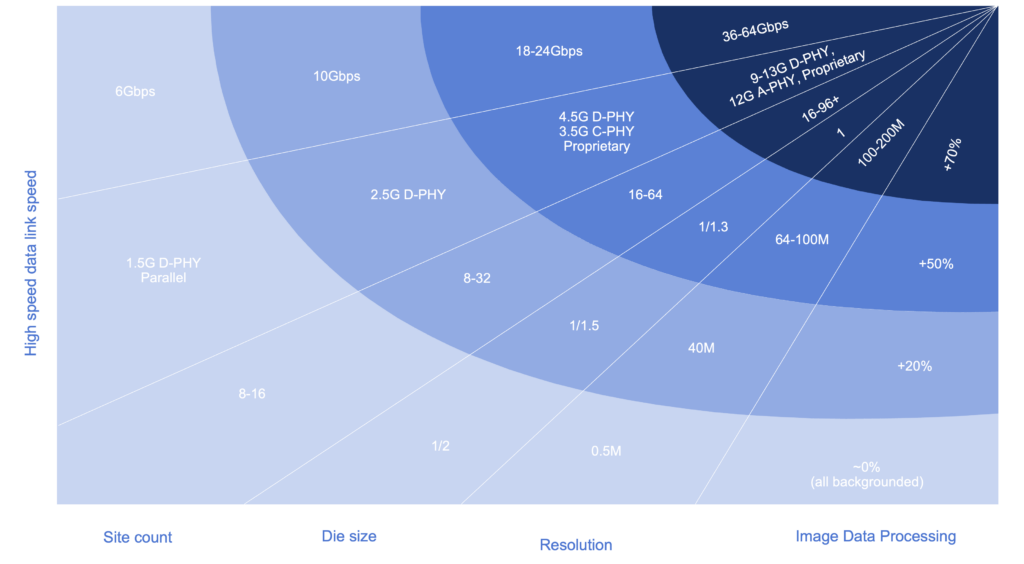
So what does this increase in complexity and resolution mean for image sensor test? It means additional test challenges, not only in the individual segments but also that compound when taken together, as illustrated in the graphic above.
Data Transfer Bandwidth
Beginning from the top left, there is an increase in the data transfer bandwidth per device, which is the amount of data that needs to be moved from the device back to the image data processor. The test system must be designed in a way that the data transfer time doesn’t impact the throughput of the test cell. The key components are the capture time, image processing time and data transfer time.
High Speed Interfaces
Add to that the need for higher-speed interfaces. The protocols that are defined and used in these sensors are changing and manufacturers are implementing different techniques to increase the bandwidth of the data that they can support, which is important both for extracting image data and also the power budget of the system. The interface wants to be ‘on’ as short a time as possible, which means extracting the data as quickly as possible and then returning to a low power mode. Today most sensors are still in the 2.5G C- and D-PHY range for MIPI for mobile, but the 4.5G D-PHY and 3.5G C-PHY standards have been available for a while and are increasingly being adopted in products.
There are many different interfaces servicing the image sensor market and that number is expected to continue to increase over time. MIPI standards will continue to evolve to meet market needs. C-PHY and D-PHY will persist in mobile. A-PHY and ASA will expand in automotive. Additionally, the emerging applications outlined above will continue to grow and become a larger part of the total market over time, and those often require different interfaces to communicate with the device. This proliferation of existing and new higher-speed protocols is creating unique test challenges.
Site Count
In mobile in particular, and to a certain extent as well in automotive, there’s a push to increase site count. Higher site count can enable higher throughput with a tester designed for this purpose. The key elements of image sensor requirements are high density instrumentation, configurable and high performance image data processors (IDPs), the ability to illuminate a high number of devices simultaneously, and a test system architecture that minimizes the per site overhead (PSO)
Die Size
Working against site count, specifically in the mobile market where sensors are high resolution, is the increase in die size. In image sensor test, the area being tested is limited to the size of the illuminator and the size of the die, which can limit site count. Additional factors, such as small focal lenses on the probe cards that require more space between individual die (like a skip die pattern) can limit site count further. Compounding this challenge is that the touchdown efficiency is generally reduced as the illuminated area increases. Die size is increasing due to the increase in resolution. Image sensor pixel technology will improve, enabling the required dynamic range to be achieved with smaller pixels. This will result in smaller and less expensive die, enabling higher site count. Test systems must be designed to efficiently test today’s devices, as well as devices that will emerge as the pixel size challenge is addressed..
Resolution
When resolution increases, test time increases. Image data processing time is directly related to the amount of data captured per image. For example, a 48 megapixel sensor will generate four times as much data per image as a 12 megapixel sensor. Increasing resolution requires that test systems regularly introduce newer and faster image data processors, support higher speed interfaces, and ensure that image data is efficiently moved from the capture instrument to the IDP.
Testing the Image Sensors of the Future
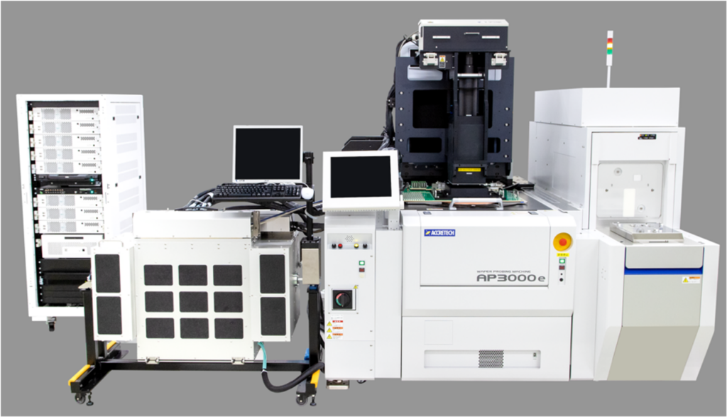
Image data processing as a percentage of total test time is increasing due to the increase in resolution while other tests remain (more or less) the same. This increase in test time can have a negative effect on the throughput of the test cell but Teradyne has invested heavily, and will continue to invest, in the IP750 platform, which has more than 2000 systems in use today, representing approximately 80% of the worldwide test capacity. In 2022, Teradyne introduced the IPQ8, an image sensor focused version of the UltraFLEXplus, that supports up to 20G serial interface sensor testing, and in 2023, Teradyne will introduce our next generation IDP, the IPG7 and new instruments supporting simultaneous combo testing of 4.5Gbps D-PHY and 3.5Gsps C-PHY.
Testing C- and D-PHY is complicated today because it either requires two passes or the addition of switches on the loadboard to switch the interface between the C- and D-PHY. In many cases, with Teradyne’s ICMCD instrument, if the device pin out conforms to a certain rule set, both C- and D-PHY can be tested without switching – a huge advantage.
Additionally, a rear shift docking system is now available for the IP750, which supports a larger illuminator space, 150 by 160 mm illuminator – half of the size of a typical 300mm wafer. Rear shift docking moves the illuminator outside the test head to support a larger illuminator and higher site count.

Going forward Teradyne’s roadmap will focus on both improving image processing time and implementing new interfaces, with the goal of shortening development time and enabling industry leading throughput.
As image sensors proliferate, being used in more and more applications, and they become increasingly complex with higher resolution, faster interfaces for data processing and better dynamic range, the effects on test can be significant. The additional test vectors coupled with the constant requirement to reduce test time and cost, mean novel solutions must be developed to maintain quality, throughput and volume. With solutions for nearly every image sensor available today and a focus on innovation to ensure the image sensors of tomorrow can be tested, Teradyne is a trusted and valued partner to our image sensors partners around the world.
Contact us to learn more about Teradyne’s automated test equipment for image sensors.
Tom Chambers is a product manager for the Image sensor segment at Teradyne, where he is responsible for the development of new image sensor products. Prior to this role, Tom held various roles in marketing and applications engineering at Teradyne. He holds a Bachelor of Science degree in electrical engineering from the University of Illinois at Urbana-Champaign.
